FPGA Development with wujian100 SoC - Part One: Bitstream Generation
Generate wujian100 SoC Bitstream file in windows with Vivado 2018.3
FPGA Development with wujian100 SoC
Part One: Bitsream Generation
Author: 加一(Jiayi)
Something to say
Recently I participated in a contest named Integrate Circuit Innovation Contest which requires me to use WJ100 developed by Ali Inc. team t-head and an FPGA develop board with Xilinx XC7A200TR3B Core. It’s not my first time to cope with FPGA but still, I find it difficult to interpret Verilog Code and make the FPGA works. Luckily, with the help of WJ100 Sdk and CDK(C-sky Develop Kit) which was developed by Ali Inc., we could jump the Verilog and long waiting synthesizing part directly to use the pre-setted circuit and easy writing C to develop.
About WJ100
T-Head’s Wujian SoC Platform utilizes the cloud-terminal-integration design philosophy that fuses software and hardware. Full-stack integration of chips, operating systems, and algorithms enable customers to develop chip products that can be mass-production.
Low power consumption: User-defined power consumption scenarios, with the standby power consumption of less than 1uA, and operating power consumption of less than 100uA/MHz
According to the official sites of Pinhead Inc., WJ100 is a low cost and high power efficiency SoC, which barely means that it could be easily deployed on any chips and consumes lower power.
However, as I talked before, it is an open-source project and as I believed, the real function of this SoC is to simplify the use of FPGA and to offer the developer a brand new way to develop: integrate Soc and FPGA to deal with some projects which require both power efficiency and fast steady frequency.
- related websites t-head
How to use WJ100 SoC
This tutorial is for those who utilize Vivado to generate bitstream file and CDK to develop your projects with Windows. This tutorial is for those who utilize Vivado to generate bitstream file and CDK to develop your projects with Windows.
-
For Part 1 Bitsream Generation please refer to Part_1_Bitstream_Generation.
-
For Part 2 CDK Toolkit and wujian100 SDK please refer to Part_2_CDK_Toolkit&Wujian100_SDK.
-
For Part 3 Start a New Project on CDK please refer to Part_3_Start_a_New_Project_on_CDK
-
For Part 4 Hello World please refer to Part4_Hello_World
-
For Part 5 GPIO please refer to Part5_GPIO
-
For Part 6 UART please refer to Part6_UART
-
For Part 7 TIMER please refer to Part7_TIMER
-
For Part 8 Interrupt please refer to Part8_VIC
Part 1 Bitstream Generation
-
clone wujian100_open project into your computer with git bash or GitHub. Or just download and unzip it.
-
As demonstrated by readme.md in wujian100_open repo, the structure of this repo is as following
 Directory Structure
 |--Project                //open source project work directory
 |--riscv_toolchain      //tool chain install directory download from t-head.cn
 |--wujian100_open       //wujian100_open project get from github
     |--case               //test case example for simulation
     |--doc                //wujian100_open user guide
     |--fpga               //FPGA script
     |--lib                //compile script for simulation
     |--regress            //regression result
     |--sdk                //software design kit
     |--soc                //Soc RTL source code
     |--tb                 //test bench
     |--tools              //simulation script and setup file
     |--workdir            //simulation directory
     |--LICENSE
     |--README.md
according to this structure what we need for bitstream generation is in the
socandfpgafolder.- THE FOLLOWING PARTS 3. – ARE INDIRECTLY INTERPRETED FROM wujian100_open的FPGA实现——如何用vivado生成wujian100_open的比特流文件 CHINESE DEVELOPER COULD DIRECTLY LOOK UP IN THIS PAGE. THANK Lianglonghui FOR HIS SHARING
-
Prep your Vivado, I use Vivado 2018.3, but as I believe the newer or older versions could also work, the demonstration all runs in Vivado 2018.3 HLX Edition and Windows 10.
-
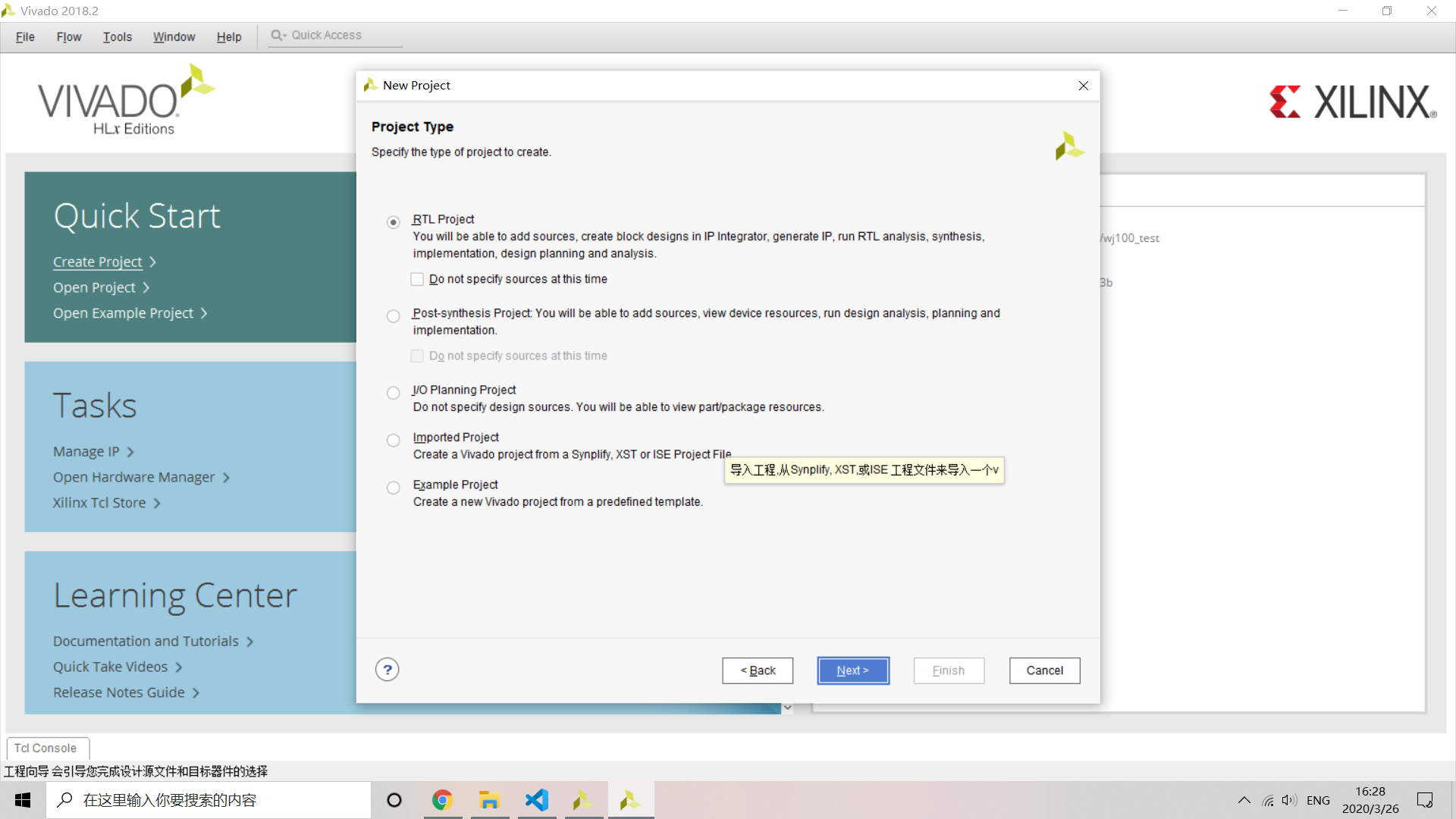
Open your Vivado and create a new RTL project.
-
Add source directory
./wujian100_open/socandwujian100_open_fpga_top.vin directory./wujian100_open/fpga. -
Check
Scan and add RTL files into project,copy source into project, andadd sources from subdirectory.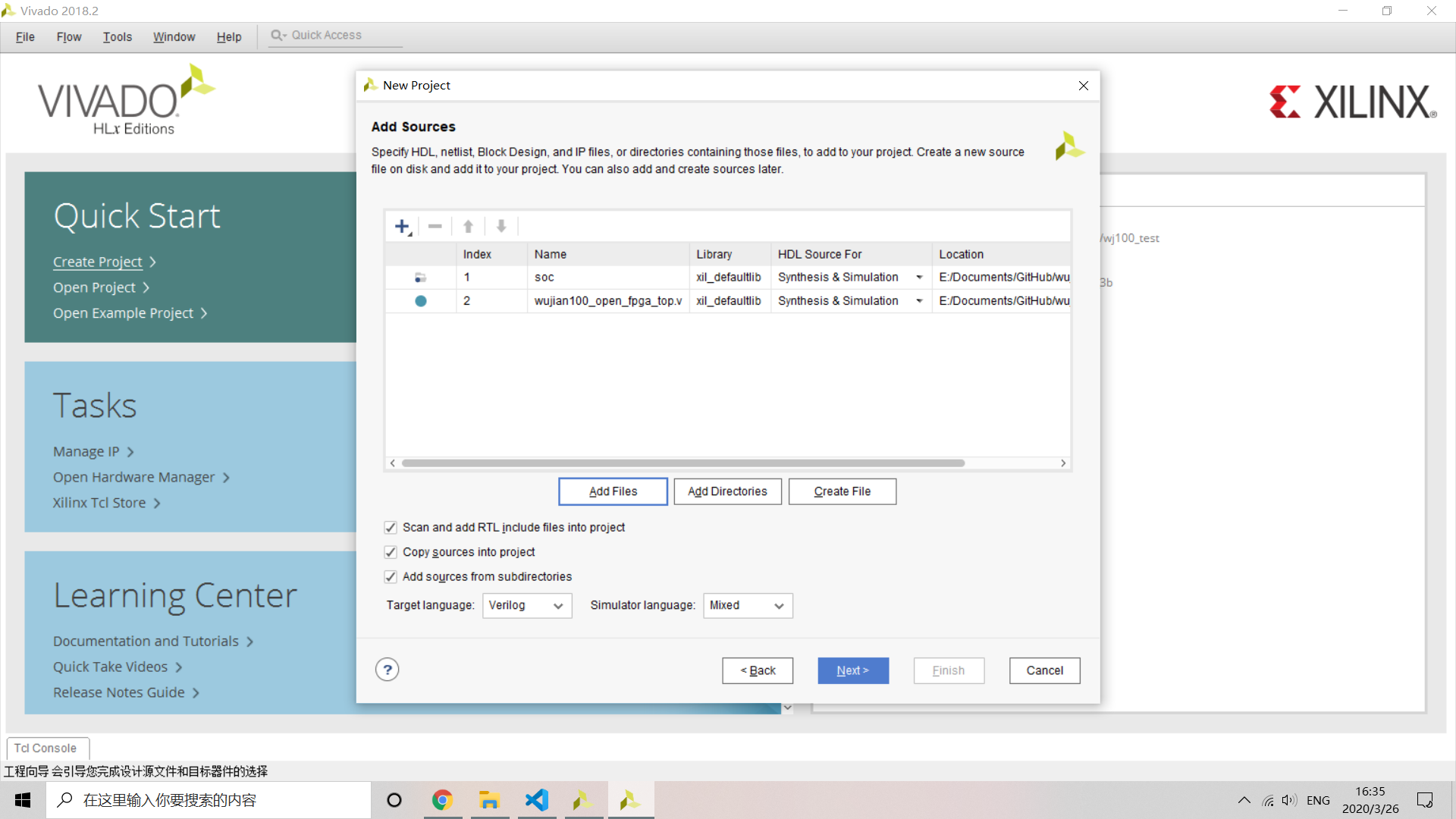
-
Add constrain file
XC7A200T3Bin directory./wujian100_open/fpga/xdcand checkcopy constrain into project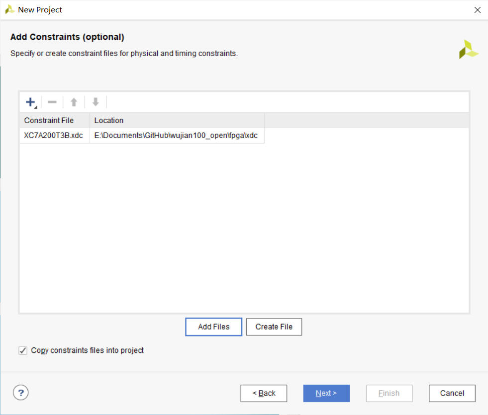
-
Search device
XC7A200TFBG484-2LinPartmenu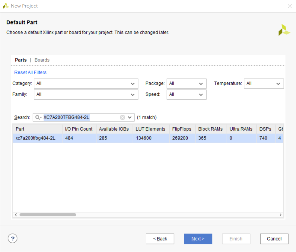
-
Finish create and the guide should be like
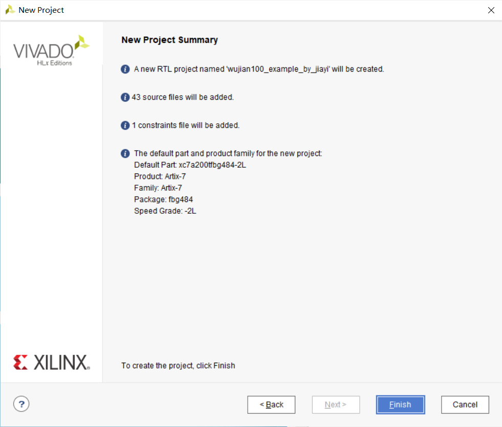
-
After Vivado has created the project, as we could see, there might be 4 syntax error files, which is due to the wrong file type. Hence we should correct it manually by right click every error file and choose
source file propertyand change its property intoverilog headeras following.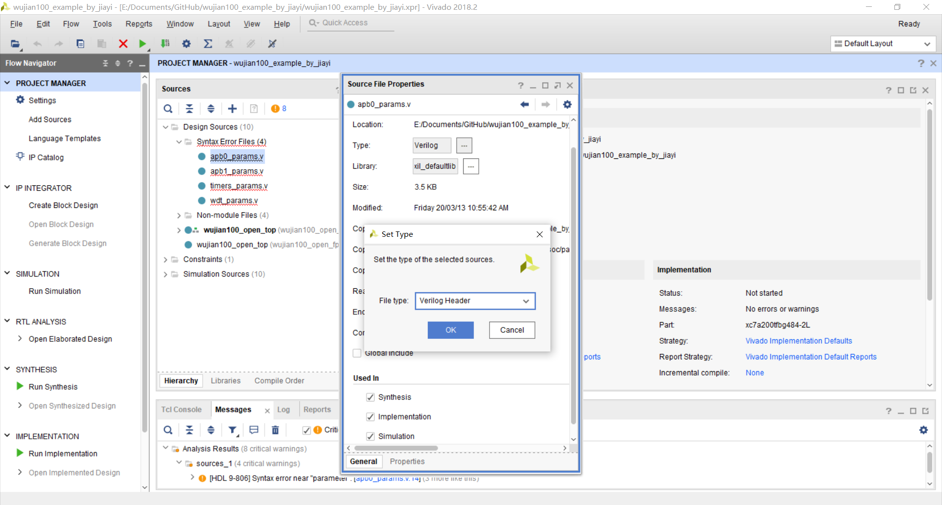
-
As we add our sources by adding a directory, we actually added a redundant source file. We need to remove the file
wujian100_open_top.v. -
After removing the file, we could set the top file
wujian100_open_fpga_top.vto be the first to compile.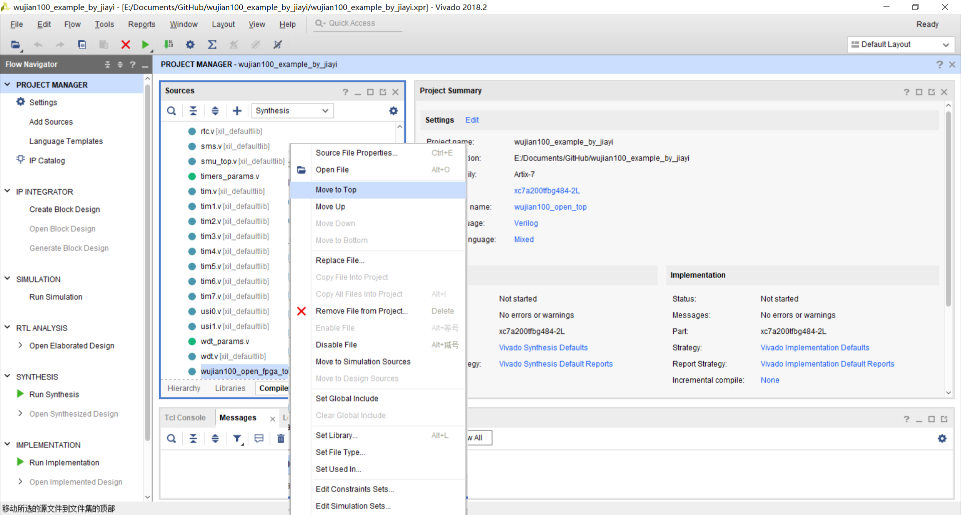
- TWO important STEP
-
Since the constrain file did not constrain the clock, we must add the following xdc code into the file
XC7A200T3B.xdccreate_clock -name {EHS} [get_ports PIN_EHS] -period 50 -waveform {0 25} create_clock -name {JTAG_CLK} [get_ports PAD_JTAG_TCLK] -period 1000 -waveform {0 500} set_clock_groups -asynchronous -name {clkgroup_1} -group [get_clocks {EHS JTAG_CLK}] set_false_path -through [get_ports PIN_EHS] #set_clock_groups -name {Inferred_clkgroup_0} -asynchronous -group [get_clocks {wujian100_open_top|PAD_JTAG_TCLK}] set_property ASYNC_REG TRUE [get_cells {x_aou_top/x_rtc0_sec_top/x_rtc_pdu_top/x_rtc_clr_sync/pclk_load_sync2_reg}] set_property ASYNC_REG TRUE [get_cells {x_aou_top/x_rtc0_sec_top/x_rtc_pdu_top/x_rtc_clr_sync/rtc_load_sync2_reg}] set_property ASYNC_REG TRUE [get_cells {x_aou_top/x_rtc0_sec_top/x_rtc_pdu_top/x_rtc_clr_sync/pclk_load_sync1_reg}] set_property ASYNC_REG TRUE [get_cells {x_aou_top/x_rtc0_sec_top/x_rtc_pdu_top/x_rtc_clr_sync/rtc_load_sync1_reg}] set_property ASYNC_REG TRUE [get_cells {x_cpu_top/CPU/x_cr_had_top/A15d/A74/A10b_reg}] set_property ASYNC_REG TRUE [get_cells {x_cpu_top/CPU/x_cr_had_top/A15d/A74/A18597_reg}] set_property ASYNC_REG TRUE [get_cells {x_cpu_top/CPU/x_cr_had_top/A15d/A1862d/A10b_reg}] set_property ASYNC_REG TRUE [get_cells {x_cpu_top/CPU/x_cr_had_top/A15d/A1862d/A18597_reg}] set_property ASYNC_REG TRUE [get_cells {x_cpu_top/CPU/x_cr_had_top/A15d/A75/A10b_reg}] set_property ASYNC_REG TRUE [get_cells {x_cpu_top/CPU/x_cr_had_top/A15d/A75/A18597_reg}]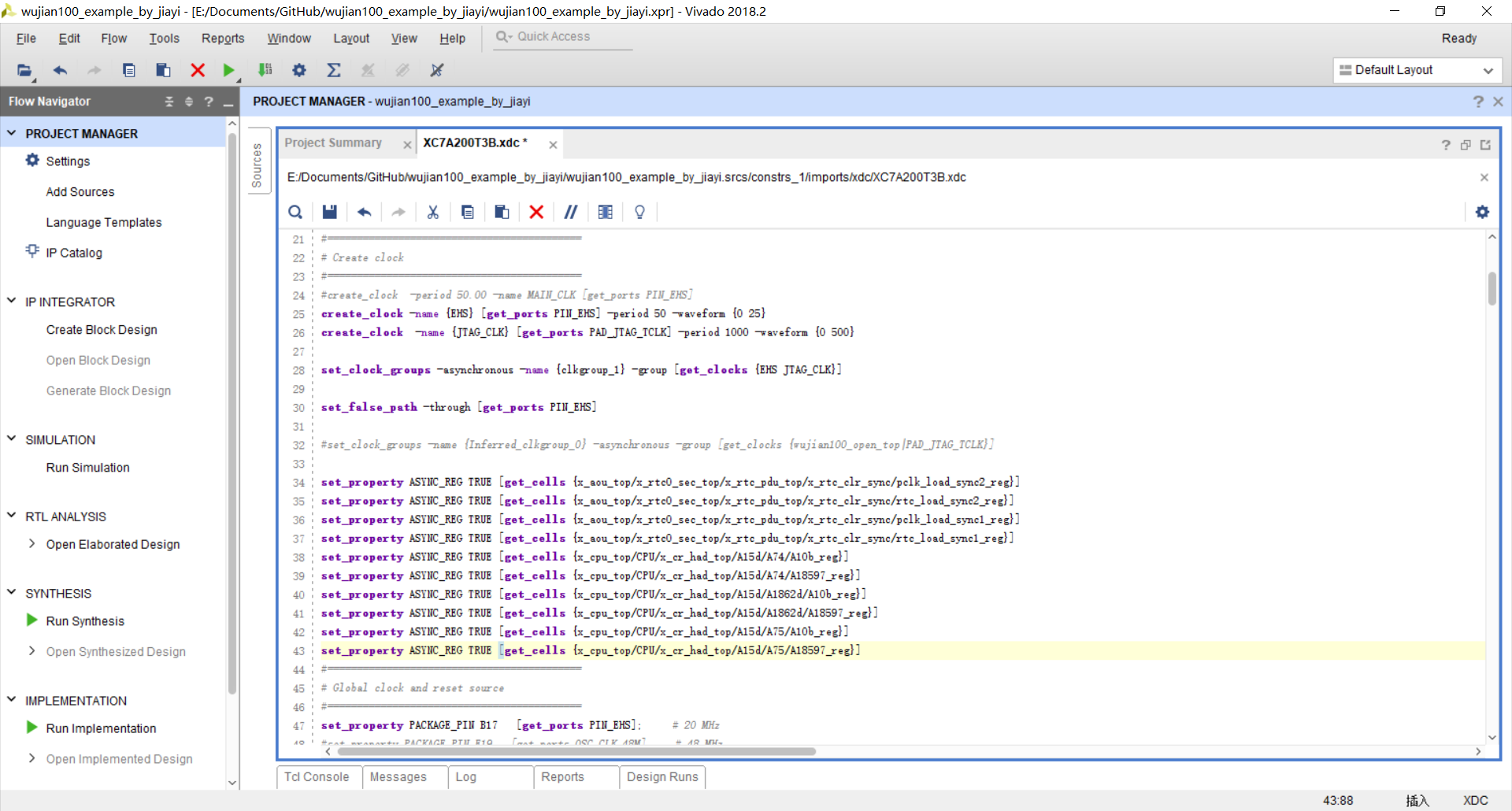
-
change one name from
get_nets PAD_JTAG_TCLK_cintoget_nets PAD_JTAG_TCLK. i.e.,# set_property CLOCK_DEDICATED_ROUTE FALSE [get_nets PAD_JTAG_TCLK_c] into set_property CLOCK_DEDICATED_ROUTE FALSE [get_nets PAD_JTAG_TCLK] -
Generate Bitstream and watch two sets of Rick and Morty since it costs me 31 minutes to finish the bitstream writing.
-
Finally we receive the success message. Find your
wujian100_open_top.bitfile in directory./{your_project_name}.runs/impl_1}. And change the file name into cfg.bit. -
Copy your cfg.bit file into your FPGA. Check if it works.(First-time configuration may fail. Just press re-prog one another time)
-
___________________________________________________________________
This article might be updated in the future, please refer to the original site: https://shieldjy.github.io/post/FPGA-Development-with-WJ100-SoC-P1.html , to avoid misleading by false or out-dated information, and to have a better reading experience.
If you would like to follow my latest blog, please click RSS Subscribe。
___________________________________________________________________
 This work is licensed under a
Creative Commons Attribution-NonCommercial-ShareAlike 4.0 International License.
This work is licensed under a
Creative Commons Attribution-NonCommercial-ShareAlike 4.0 International License.
It is widely welcomed to copy and redistribute the material in any medium or format as well as remix, transform, and build upon the material, but make sure you have referred Jiayi (And include the url: https://shieldjy.github.io ).
However, You may not use the material for commercial purposes. If you remix, transform, or build upon the material, you must distribute your contributions under the same license as the original.
If there is any problem, please contact me for further information. (lijiayi19971127@hotmail.com)