Dynamic Random Access Memory
Research for DRAM.
1. What is DRAM
Dynamic random-access memory (DRAM) is a type of random access semiconductor memory that stores each bit of data in a memory cell consisting of a tiny capacitor and a transistor, both typically based on metal-oxide-semiconductor (MOS) technology.wikipedia
2. Structure of DRAM Cells
Figure 2.1 DRAM Cell Structure
From figure 2.1, as we could see, DRAM is actually a 1T1C(one transistor and one capacitor) structure. Writing process is accomplished by selecting bit line 1 and word line 2 thus pull up/down the voltage of capacitor 4. Firstly, data is stored by applying high voltage to both word line 2 and bit line 1. And then data is stored by applying a low voltage to the word line 2 and trapping the charge on the storage capacitor. Subsequently, the data is accessed by applying a high voltage to the wordline to make FET work in depletion mode, conduction bitline and capacitor, so that the voltage on the bit line 1 could be sensed. Then Word line or Bit line is turned to be Low Voltage Level to config next cell so that FET works in cut off mode and thus the voltage level is stored in capacitor 4. When the data is read, apply a high voltage on word line 2 and thus the charges in capacitor 4 is released and could be sensed in bit line 2.
However, this memory cell structure is volatile for two reason. For one, the voltage level of capacitor is hold due to its capacity of charges, but the charges will leak as time passed by. This process is basically due to the current leakage. And there is an important term names retention time. The retention time can be defined as the duration until the stored signal can be read out. There are several leakage current mechanisms, by which the stored signal disappears [11]. Including 1) junction leakage current from the storage node, 2) subthreshold leakage current of the transfer transistor, 3) capacitor dielectric leakage current, 4) gate induced drain leakage (GIDL) current at the storage node,5) gate dielectric leakage current, and 6) isolation leakage current between the neighboring cells. Study shows, the major leakage paths in a DRAM cell are reverse junction leakage from the storage node and gate induced drain leakage (GIDL) current [1]. For two, the reading process, the process we have discussed before, is destructive to the charge stored in the capacitor, which stands for the data. And this is due to its 1T1C structure.
Hence, Dynamic Random Access memory, although cheap to manufacture (in contrast to early stage solid states hard drive), fast read - write process and almost unlimited read-write cycles, has a fatal problem. It’s volatile feature. But nowadays there are problems with solid state memories and also with traditional DRAM. So there are quite a few researches that deal with the novel structure of DRAM and novel FET(Field Effect Transistors).
3. Latest researches on DRAM
Volatile
Volatile memory means the storage device will lose its data once the power is cut off.
Float Body Cell (FBC) Structure for 1T-DRAM
Although the principle of 1T1C DRAM is relatively simple, the capacitor in it is not that simple, for it requires a relatively large capacity of charge in its scale (around 30 fF/cell). Anyone who has some knowledge about capacitor should aware that Farad is not a small unit, 10mF capacitor could be called as “Super Capacitor” and is huge for a normal sized PCB.
Figure 3.1 a 10 Farad Super Capacitor(in contrast to a quart coin)
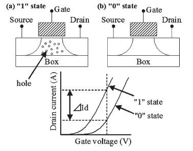
It is not difficult to imagine how large it is for a 30fF Cap in a DRAM cell. To deal with this issue, some reseachers[2]-[10] create a 1T structure, or floating-body cell (FBC) for DRAM. The FBC structure is shown in Figure 3.2. It operates as follows: When excess holes exist in the floating-body and Vth lowers, the cell state can be regarded as “1”. On the other hand, when excess holes are swept out of the floating-body by a forward bias on the body–drain junction and Vth becomes higher, the cell state can be regarded as “0”. The drain-current difference between “1” and “0” states can be sensed in the linear current region so as not to change the number of holes by the II current[2], which is an impact-ionization current used in wrting process.
 Figure 3.2 1T Structure of DRAM
In contrast to 1T1C DRAM cells, the writing process with GIDL current consume lower by four orders of magnitude of power and a write speed within several nanoseconds. According to its data, Power consumption for writing “1” could be as low as $2.4 \times 10^-8$ Watt [2]. Furthermore, the reading process is non-destructive. However, this novel method is not widely taken for it has fatal weakness: its writing process is heavily relied on II current and 1 and 0 states detected by current. This is not what we truly like in an operating device. Since millions of cells could produce a huge current what requires the impedance of the whole device must be extradentary low, which is unachievable. Moreover, threads of devices are not designed to drain current for it is designed with a high pull up resistor to increase its impedance so as to increase its capability of voltage detection. The 1T DRAM could not be compatible with most common device.
Non-Volatile
Non-volatile memory (NVM) means the storage device will not lose its data after a relatively long time of cutting off. The time for how long its data could remain is called retention time and is an important measurement for non-volatile memory.
Non-volatile memory has been widely used in SRAM which is a high speed but large cell structure and Flash which is low speed but high density.
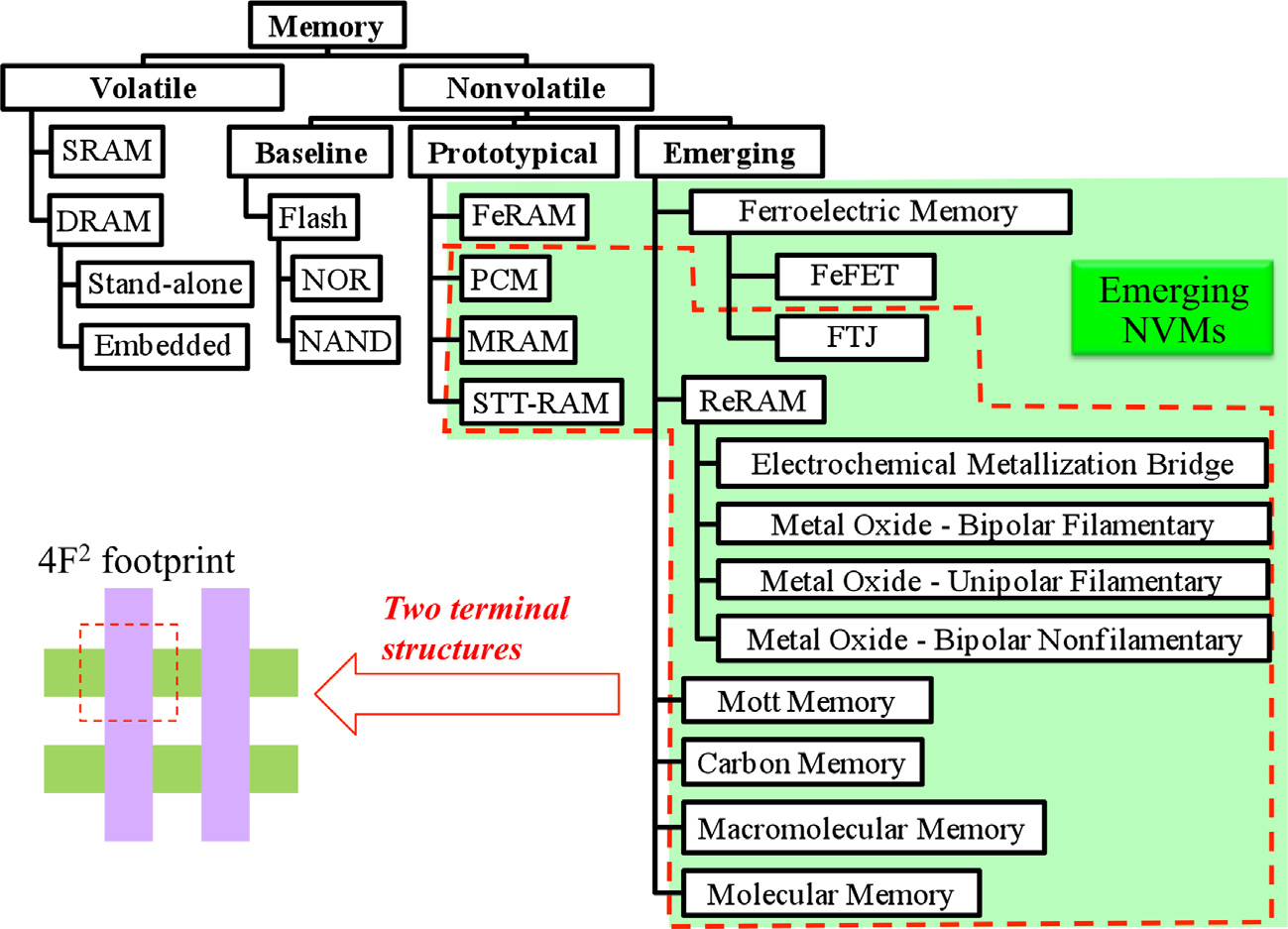
 Figure 3.3 Memory taxonomy from the 2013 ITRS Emerging Research Devices (ERD) chapter[12]
Typically, there are several types of Non-Volatile memory cells, shown as right part in Figure 3.3. Categorized by cell technology, for instance, phase change memory, know as PCM, spin-transfer-torque random access memory, known as STTRAM, resistive random access memory, known as RRAM and ferroelectric field- effective-transistor memory, known as FeFET Memory.
Categorized by material used in the cell, there are inorganic and organic way. Among those, inorganic non-volatile memories have now been put into industrial manufacture, for instance Ferroelectric Random Access Memory (FRAM).
However, in this article, NVM categorized by organic and in-organic way will be discussed.
Inorganic Non-Volatile Memory Cells
Organic Non-Volatile Memory Cells
Reference
[1] u, J. and K. Aflatooni (2006). Leakage Current in DRAM Memory Cell. 2006 16th Biennial University/Government/Industry Microelectronics Symposium.
[2] Yoshida, E. and T. Tanaka (2006). “A capacitorless 1T-DRAM technology using gate-induced drain-leakage (GIDL) current for low-power and high-speed embedded memory.” IEEE TRANSACTIONS ON ELECTRON DEVICES 53(4): 692-697. Sasaki, N., et al. (1978). Charge pumping SOS-MOS transistor memory. 1978 International Electron Devices Meeting, IEEE.
[3] Tack, M. R., et al. (1990). “The multistable charge-controlled memory effect in SOI MOS transistors at low temperatures.” IEEE TRANSACTIONS ON ELECTRON DEVICES 37(5): 1373-1382.
[4] Wann, H.-J. and C. Hu (1993). A capacitorless DRAM cell on SOI substrate. Proceedings of IEEE International Electron Devices Meeting, IEEE.
[5] Okhonin, S., et al. (2001). A SOI capacitor-less 1T-DRAM concept. 2001 IEEE International SOI Conference. Proceedings (Cat. No. 01CH37207), IEEE.
[6] Fazan, P., et al. (2002). Capacitor-less 1-transistor DRAM. 2002 IEEE international SOI conference (Williamsburg VA, 7-10 October 2002).
[7] Ohsawa, T., et al. (2002). “Memory design using a one-transistor gain cell on SOI.” IEEE Journal of Solid-State Circuits 37(11): 1510-1522.
[8] Inoh, K., et al. (2003). FBC (floating body cell) for embedded DRAM on SOI. 2003 Symposium on VLSI Technology. Digest of Technical Papers (IEEE Cat. No. 03CH37407), IEEE.
[9] Yoshida, E. and T. Tanaka (2003). A design of a capacitorless 1T-DRAM cell using gate-induced drain leakage (GIDL) current for low-power and high-speed embedded memory. IEEE International Electron Devices Meeting 2003, IEEE.
[10] Shino, T., et al. (2004). Highly scalable FBC (floating body cell) with 25nm BOX structure for embedded DRAM applications. Digest of Technical Papers. 2004 Symposium on VLSI Technology, 2004., IEEE.
[11]Hamamoto, T., et al. (1998). “On the retention time distribution of dynamic random access memory (DRAM).” IEEE TRANSACTIONS ON ELECTRON DEVICES 45(6): 1300-1309.
[12]ITRS Emerging Research Devices Chapter, 2013.
___________________________________________________________________
This article might be updated in the future, please refer to the original site: https://shieldjy.github.io/post/Dynamic-Random-Access-Memory(DRAM).html , to avoid misleading by false or out-dated information, and to have a better reading experience.
If you would like to follow my latest blog, please click RSS Subscribe。
___________________________________________________________________

It is widely welcomed to copy and redistribute the material in any medium or format as well as remix, transform, and build upon the material, but make sure you have referred Jiayi (And include the url: https://shieldjy.github.io ).
However, You may not use the material for commercial purposes. If you remix, transform, or build upon the material, you must distribute your contributions under the same license as the original.
If there is any problem, please contact me for further information. (lijiayi19971127@hotmail.com)